Table of Contents
Combinational & sequential functions
1. Combinational functions in ICs
Combinational logic functions are available in prefabricated MSI (medium-scale integration) chips; one chip can have more than 100 gates. Here are some digital animals in the MSI zoo.
1.1 2-input MUX
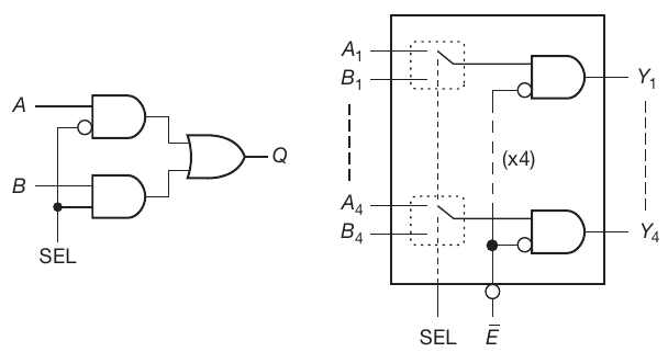
When SEL is LOW (L), A inputs are passed to the outputs; when SEL is HIGH B inputs are passed. When $\overline{ENABLE}$ ($\overline{E}$) is HIGH (H), the device is disabled and we don’t care about the inputs.
Designator: ‘157: quad 2-input select chip. ‘158: ‘157 with inverted output. ‘257: three-state outputs.'1G157: single-section MUX without EN’.
1.2 Transmission gate

Two CMOS switches in parallel, one NMOS and one PMOS. Their drains and sources are interconnected and provide the input or output, nY or nZ. And their gates are connected to the ENABLE pin nE (1E to 4E).
When nE is HIGH, either the NMOS or the PMOS is enabled and take the I to O.
When nE is LOW, both are disabled and the switch is open and no current flows.
1.3 Many-input MUX

In order to make an 8-input MUX, take transmission gates and replace the ENABLE option with a 3-input SELECT. The eight inputs can selected with 3 bits.
1.4 Demultiplexers and decoders
1.5 Full adder
1.6 Other IC functions
- Priority encoder (SN74LS148): gives the binary address of the highest-numbered input.
- Magnitude comparator (74HC85D): tells you whether for inputs A and B, $A<B$, $A=B$ or $A>B$.
- Parity generator (74HCT280D): generates odd/even parity bit during transmission and checks the parity during reception. Uses XOR gates.
2. Sequential logic
Typical sequential tasks: converting bits from serial to parallel, counting the number of 1s, recognizing pattern, controlling the state of a system with time. The output depends on both the present and past input states. Cannot be created from gates alone; some sort of memory (flip-flop) is needed.
2.1 Flip-flops
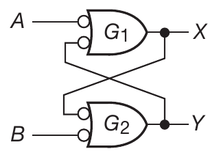
This is the most basic flip-flop, simply called latch.
Let us see how this works:
- Latch starts out RESET, X=0, Y=1, A=1, B=0. A momentary LOW is applied on A, G1 gets 0, 1 and X becomes HIGH. Latch is SET.
- Latch starts our SET, X=1, Y=0, A=0, B=1. A momentary LOW on A does not change anything.
- Latch starts out SET, momentary LOW is applied on B: Latch is RESET.
- Latch starts out RESET, momentary LOW is applied on B: Latch is SET.
| A | B | X | Y | Comments |
|---|---|---|---|---|
| 0 | 0 | 1 | 1 | Invalid condition |
| 0 | 1 | 1 | 0 | Latch SET |
| 1 | 0 | 0 | 1 | Latch RESET |
| 1 | 1 | NC | NC | No change |

S-R Latch SN74LS279ADR can be used as a switch debouncer.
2.2 Clocked flip-flops

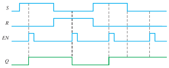
| S | R | $Q_{n+1}$ |
|---|---|---|
| 0 | 0 | $Q_n$ |
| 0 | 1 | 0 |
| 1 | 0 | 1 |
| 1 | 1 | indeterminate |
Here $Q_{n+1}$ is the output after the clock pulse and $Q_n$ that before the pulse.
2.3 D dlip-flops
By far the most popular kind of flip-flops.

When D is 1, Q is 1 and vice versa.
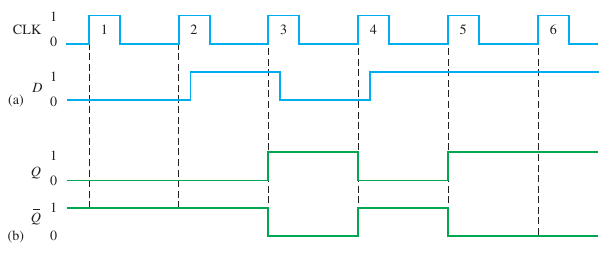

While CLK is HIGH, gates 1 and 2 are enabled, forcing master to have same output as D; the slave is disabled so it retains its previous state.
When the CLK goes LOW, inputs to the master are disconnected and the slave gets its inputs from the outputs of the master. This is negative edge triggered.
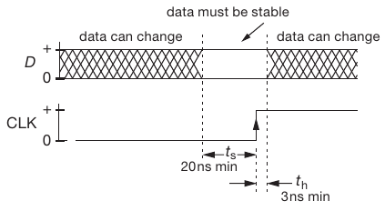
Data and clock timing
2.4 J-K flip-flops
A positive edge triggered J-K flip-flop.

| J | K | $Q_{n+1}$ |
|---|---|---|
| 0 | 0 | $Q_n$ |
| 0 | 1 | 0 |
| 1 | 0 | 1 |
| 1 | 1 | $Q'_n$ |
If J and K are complements, Q will get J input at the next clock edge.
2.5 Three uses of flip-flops

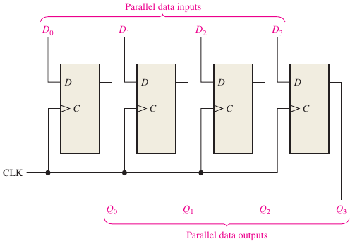
Parallel data storage

Frequency divider
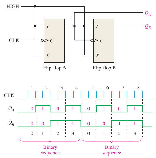
Counter
2.6 Memory and gates
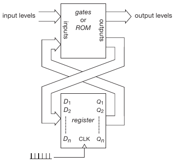
The classic sequential state machine. A set of clocked flip-flops and combinational logic.
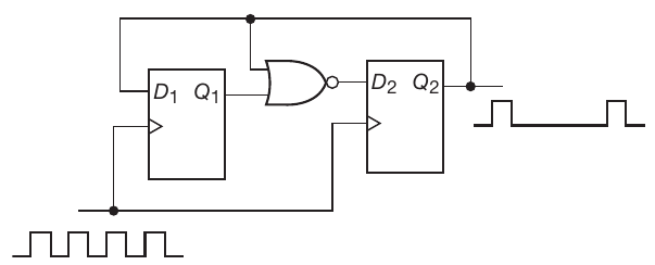
An example of a 3-state machine. First define the three states of the Q outputs.
| $Q_1$ | $Q_2$ |
|---|---|
| 0 | 0 |
| 0 | 1 |
| 1 | 0 |
Figure out what the D inputs have to be for these outputs.
| $Q_1$ | $Q_2$ | $D_1$ | $D_2$ |
|---|---|---|---|
| 0 | 0 | 0 | 1 |
| 0 | 1 | 1 | 0 |
| 1 | 0 | 0 | 0 |
Now figure out the combinational logic needed. Here $D_1=Q_2$ and $D_2=(Q_1+Q_2)'$. So we need a NOR gate.
But what happens if somehow you get $(Q_,Q_2)=(1,1)$? The divider will be stuck. So these invalid states have to be excluded. We can use state diagrams for this purpose.
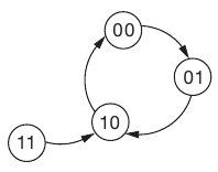
2.7 Counter
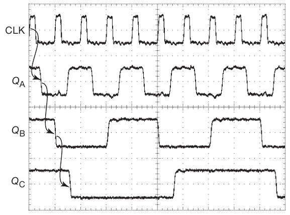
A 3-bit ripple counter / divide by $2^n$:
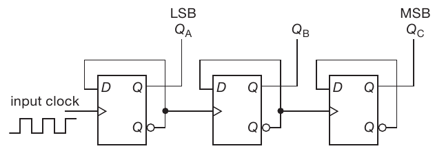
And its timing diagram:
A 3-bit synchronous binary counter:
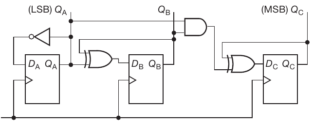
And the timing diagram:
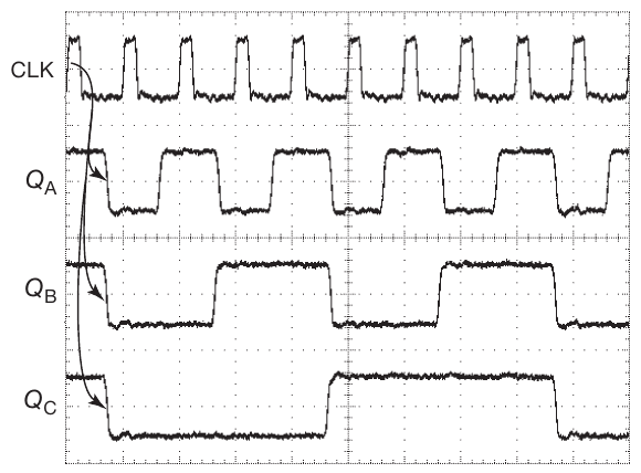
2.8 Shift register
Serial in Serial Out:
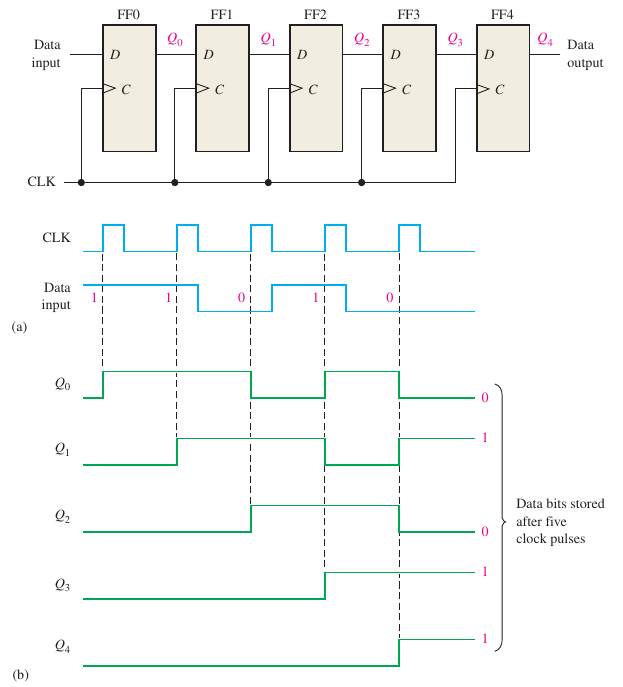
Serial in Parallel out:

Parallel in Serial out:
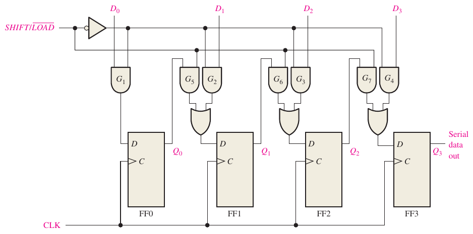
Parallel in Parallel out:
